
Ink mark inspection device
It measures the area of ink marks stably with almost no influence from patterns! A special optical system that accommodates various wafer types.
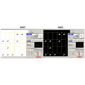
The device is an automatic inspection system that can measure the area of ink marks stably with minimal influence from patterns. It uses a special optical system that brings out ink with stable detection capability for various wafer types. Measurement can be performed simply by setting the brightness values of the illumination and the binarization level for each wafer type, and it communicates with the prober via GPIB. Additionally, a device that operates with a dedicated XY stage instead of a prober can also be manufactured. 【Features】 ■ Special optical system that brings out ink for various wafer types ■ Stable measurement of ink mark area with minimal influence from patterns ■ Simple setup to determine the brightness values of the illumination and the binarization level ■ Automatic inspection possible via GPIB communication ■ A device with a dedicated XY stage can also be manufactured *For more details, please download the PDF or feel free to contact us.
- Company:アローズエンジニアリング
- Price:Other
